The most important part of a typical solar cell system is the semiconducting material of the solar panel itself. Semiconductors, along with metals, insulators and semi-metals, are basic building blocks of Nature. They possess very distinctive electronic characteristics which make them ideal for solar applications. One of their significant features is the ability to convert the incident sun light into electric current.
The light photons of certain energy of the solar spectrum are capable of exciting electrons from their normal position within the semiconductor, effectively producing electron-hole pairs (a hole in this case is the lack of electron within the atom). Next, the electron-hole pairs are separated with the help of semiconducting junctions – special micro designs that effectively enable accumulating of electric carriers. The junctions are usually made by doping of the pure semiconductor with the aim to produce hole rich and electron rich materials (p and n-type). The photo induced electrons are afterward being directed toward the external circuit via the contacts on the front and rare parts of the panel.
Silicon is the main material for solar cell production. Currently, silicon technologies hold the largest market share in this industry. In the attempt to improve the overall features and lower the costs of production, there is a substantial effort to include also CdTe, GaAs, InP, CIS (chalcopyrite) and other types of crystalline materials in the process of solar cells manufacturing. Usually, crystalline silicon (c-Si) is used in form of wafers, whereas the other compounds are designed as thin films. Thin films are materials of choice for inexpensive and flexible solar panels. There is a line of solar research directed toward modeling the inherent band gaps. It is well known that various materials with specific band gaps respond differently to different light frequencies of the solar spectrum. Many of those promising technologies are showing great potential for large scale applications
Single crystalline silicon, as compared to the thin films, has to be prepared in relatively thick layers. This involves crystal growth and sawing, which means that the wafers are produced in complicated and energy demanding processes. The wafers need to possess very regular structure patterns and to be of high purity. After the preparation phase, in order to make the junctions, they are usually doped in a controlled manner with other chemical elements. The good efficiency and stable output means that this is the material of choice for many practical applications.
Poly-crystalline or multicrystalline silicon technology stands right next to the use of single crystalline materials. Despite the fact that the wafers made out of poly-crystalline silicon show diminished efficiency, the general trend is to shift toward this type of solar cell technologies.
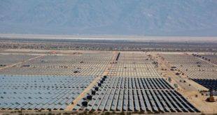
The c-Si solar cells are capable of delivering voltage of 0.5 Volts. Since this is a quite low value, the cells need to be assembled together to produce modules of higher voltage. In such a way, solar modules are obtained ready to be used in, for instance, solar chargers for laptops, smaller home systems, or larger solar power fields.
Other technologies are constantly being researched in the attempt to lower the costs of production and/or increase the solar cell efficiency. Thin films can have orders of magnitude lower thickness and can easily cover substantially larger surface areas. This makes them ideal to increase the productivity and lower the production costs. They can be produced virtually using any semiconductor materials, such as for example amorphous silicon (a-Si), cadmium telluride, gallium arsenide, or copper indium diselenide.
The a-Si technology is the most advanced thin films technology for solar cells production. The amorphous solar cells are usually layered devices with cells built on top of the other cells. Less efficient as they are, the amorphous silicon panels are more affordable due to the reduced material and larger substrates. They position themselves in the market of lower power systems and consumer electronics.
Despite their favorable performances, some thin film materials, such as cadmium telluride (due to the health and environmental effects of cadmium) are questionable from the point of view of safety of operation and environmental preservation.
There are several important parts of every photovoltaic system, but the most crucial aspect is the solar panel itself. The key to understanding the solar cell performance is to consider the underlying technology and how it is applied in practice. In spite of the considerable progress in device manufacturing and using of solar energy, there is much room for improvements for this clean, free, and sustainable energy source.
 Alternative Energy HQ solar power for homes, wind energy, and bio fuel issues


